8585 INTEGRATED STEREO AMPLIFIER, 2006.
Updated January 2018.
Download the new page to replace the page from 2006. The new
page has OPT
information and a couple of re-drawn schematics.
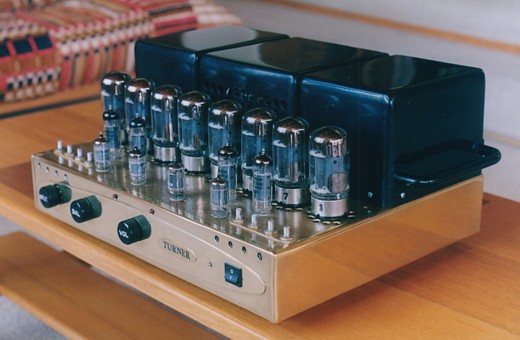
Picture 1. 8585 Amplifier in 2004 with 8 x GE 6550A.
Contents of this page....
Picture 1. 8585 Amplifier.
Fig 1. 8585 schematic input and driver amp stages.
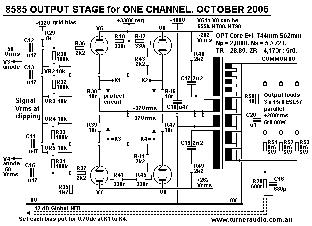
Fig 2. 8585 schematic; output stage each channel.
General description, how all circuits work, tube
choices, NFB.
Table 1. Maximum AB Po vs load RL.
Graph 1. ESL57 Z and input power.
Amp sensitivity.
Fig 3. 8585 schematic Power supply.
Many more facts about 8585.
Graph 2. 8585 Po vs Sec RL.
Graph 3. Harmonic THD spectra for 8585, 4 x KT90 per
channel.
Graph 4. Harmonic spectra for 8585 with Vol control at
max
Graph 5. THD for 8585 for 6550 in 2004, and KT90 2006.
Graph 6. THD of SE 12AU7 preamp in 8585, 2006.
Graph 7. THD for 8585 measured in 2004, 4r0 t0 8r0.
Fig 5. 8585 basic shunt NFB in preamp.
Fig 6. 8585 basic GNFB in power amp.
Graph 8. Loadline analysis for 4 x KT90 PP with 12.5%
CFB.
Picture 2. 8585 view of under-chassis space filled with
parts.
Fig 7. OPT-4B 100W PP CFB / UL for 4k0 : 1r9, 3r3, 7r5.
Fig 7 is slightly better OPT than used in 8585 in 1995.
Fig 8. 8585 schematic 2004 for input and power amp.
-----------------------------------------------------------------------------------------------------------------------------
Use of the 8585 amp without reading
all these notes is possible but
YOU MUST READ ABOUT THE BIAS
ADJUSTMENT AND FAULT INDICATION OR YOU WILL
HAVE UNWANTED INTERRUPTIONS TO YOUR MUSIC.
THE REMOVAL OF THE BOTTOM COVER OR TOP TRANSFORMER COVERS
EXPOSES
ANY PERSON TO POTENTIALLY DANGEROUS AND LETHAL VOLTAGES,
SO PLEASE
DON'T DO IT, UNLESS YOU ARE AN EXPERIENCED TECHNICIAN !
-----------------------------------------------------------------------------------------------------------------------------
Fig 1. 8585 schematic input and driver amp stages.
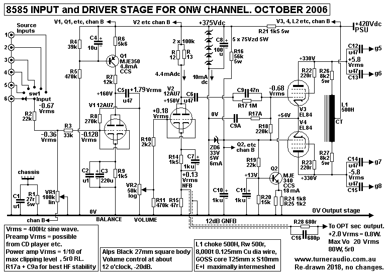
Fig 2. 8585 schematic output stage each channel.
8585 General Description.
The basic design of the push-pull 8585 was conceived in 1995,
following several years of trials with
various PP topologies to get the most accurate, dynamic, and
subjectively pleasing sound, along
with the best measurements possible with the least use of
corrective circuitry known as global NFB.
The fundamental output stage circuit design of the 8585 is
based on the use of beam tetrodes or
pentodes with renowned Acoustical Connection, famously
exploited Peter Walker in the 1950s in
Quad II amplifiers, and continued in the much later Quad-II-40
amps with the same circuit by Andy
Grove, and in Quad 80 amps.
The performance of my 8585 output transformers is a lot better
than anything built for Quad-II,
Quad-II-40.
The October 2006 version 8585 is an integrated amplifier, with
6 switched line level inputs, balance
control, line level SET preamp amp, and volume control.
Incremental improvements since 1995 evolved the present fine
sounding amplifier.
The only change to the 8585 schematic was in 2011 in
PSU where the Eg2 shunt regulator
using 4 x 75V zener diodes in series was replaced by regulator
shown in the revised PSU in Fig 3
below. The original 4 x 75V series zener diodes were found to
change their zener voltage to less
than the 75V nominal value, probably from repeated heat cycles
after turn on where the regulator
passes maximum Idc before some Idc goes to screens when tubes
heat up.
Tube Choices
There are presently 4 x KT90 output tubes per channel, but the
circuit allows the use of all the main
octal based output tubes KT120, KT90, KT88, 6550, EL34, 6CA7,
KT66,6L6GC, 5881, and the
humble JJ 6V6 now used in many guitar amps.
Maximum class AB Po is 100W+ for KT120 to 35W for 6V6.
But the Eg1 bias levels should be adjusted to suit any
change of tubes so that Iadc is not higher
than 30mAdc.
For JJ 6V6 the B+ must be lowered to about +400Vdc max, Eg2
may remain at +330Vdc.
Do NOT use NOS 6V6. I recall the 8585 has a tap on HT winding
at 150Vdc for lower B+. Idle Ia
for each JJ 6V6 for should be 30mAdc. The OPT Sec is set for
Ns = 5 x 72t for 4,172r : 5r0.
The best load for 6V6 is 8r0 giving 6k6 : 8r0, so that each
pair 6V6 have RLa-a 13k3 and class
A Po for the quad = 12W, with 35W max class AB1.
Local output stage cathode feedback.
Each channel in 2006 had 4 x KT90 with two each side of the
push-pull circuit. 12.5% of primary turns
on OPT are within the cathode to 0V circuit giving local
cathode feedback, CFB. With a 5r0 load, the
12.5% of local CFB equates to about 7dB of local NFB, and the
output tubes tetrode Ra of about 30k
each at idle is reduced to 1.37k, or just slightly higher than
triode, but .
The reason for applying two lots of negative feedback,
with one lot in the form of local CFB in the
output stage and the other globally is because the local FB in
the output stage has a very good effect
on the spectral content of distortion harmonics which are
reduced to lower levels than triode or
ultralinear connection but without paying a penalty of
requiring too high a drive voltage to the output
stage tube grids. This local CFB around as short a path as
possible and most distortion reduction is in
the output stage without involving the input and driver
stages.
Only 12dB of Global NFB is needed for a total of local
CFB and global NFB is less than 20dB.
With less GNFB, it easier to achieve unconditional stability
without requiring such critical stability
R+C networks.
The 12.5% CFB has a more dramatic effect on the pure beam
tetrode mode harmonic spectra than
UL of any % value except perhaps 100% UL which is triode
connection with screens to anode
with series 220r.
The local CFB prevents considerable production of
unwanted harmonics before needing global NFB
to complete the work. The CFB mode does require a higher
maximum Vac applied to grids than UL
or even triode, but the input SE triode and EL84 triode driver
stage has been designed to easily
give about 1/3 of the usual amount of THD for the wanted Vac.
The anode B+ supply is a nominal +500Vdc but may vary
between +510V for high Mains Vac or
down to +470V with low mains, or prolonged heavy class AB Po
where B+ will sag -5% at least.
This will rarely occur because the average Po for music
without clipping on peaks is 1/10 of the
clipping Po.
Psu has 800 VA toroidal power transformer, silicon diodes, and
large value capacitors, with one filter
choke for CLC filter for B+. Eg2 screen supply is +330Vdc,
actively shunt regulated. The output
tubes have fixed grid Eg1 -Vdc bias voltage applied, all
separately adjustable, mentioned below.
V3+V4 Driver Stage is a "long tail pair" differential
amp using 2 x EL84 or 6BQ5 in triode mode with
each idle Idc = 9mAdc. The Idc is fed from B+ rail to a centre
tap on a Choke L1 500H with 8.2k from
each end of the choke to the EL84 anodes. The choke has 8,000t
x 0.125mm C dia wire on GOSS
core T25mm x S10mm. No air gap is used. It has Rw 500r approx,
but very high inductive reactance
for most of the AF band, over 150k at 50Hz. The 8k2 prevent
excessive Idc in choke winding if anodes
of EL84 are ever shunted to 0V. But below 50Hz and above
10kHz, the shunt L and shunt C of the
choke are prevented from causing phase shift with 8k2, and
although the gain of EL84 reduces
with only 8k2 load, there is negligible phase shift, so the
driver stage effectively has L+R and C+R
gain shelving networks so the margin of stability with GNFB is
more than 12dB. it means it would be
possible to increase GNFB from 12dB to 24dB, and amp would
remain stable. I did once try to
increase GNFB to 35dB GNFB, but any further increase would
cause incurable oscillations which
did not respond to normal stability networks.
MJE340 CCS for V3+4 cathodes in LTP.
V3+V4 cathodes connect together and their total Ikdc = 18mAdc.
It flows through MJE340 on a
heatsink and arranged as a constant current sink, CCS, with
effective collector impedance < 4M0.
Both EL84 have grid bias = +33Vdc from zener regulated +33Vdc
rail. MJE340 base is biased at
+13Vdc, and this keeps Vac across emitter R24+25 very low, so
therefore any Vac at collector
produces negligible Iac, and the arrangement works much better
than having a R = 3k0 from
commoned emitters to 0V, or a larger R to the -Vdc rail used
for fixed bias.
The cathode CCS forces the +current change in one EL84 to be
exactly the same as the -current
change in other EL84. This helps the production of equal +Va
and -Va swings to drive output tubes.
Only V3 grid is driven by up to 6.8Vrms. the other V4 grid is
kept at +33Vdc with no Vac.
You would fine Vk at about 3.4Vdc, and the Vgk for each EL84
is close to equal.
Many amps have an LTP driven at one grid only, with cathode R
to a 0V or -Vdc rail and two anode
R to B+. The Vac is never equal and the anode R of non driven
triode must always be increased to
equalize the Vac. The CCS eliminates the need for adjustment
and gives the lowest THD.
Most ppl just cannot figure out why the LTP works with only
one side driven. I suggest they learn
to analyse the Iac and Idc and gains, a steep learning curve
is ahead, brain must pedal hard up
this mental hill............
The CT choke allows the Vac at each end of choke to
swing higher than the supply B+, something
impossible with "normal" R feed of Idc to anodes. The 8k2 make
no difference to the operation and
very little Vac is ever across the 8k2 so the choke + 2 x 8k2
only waste a negligible amount of anode
Po. If I had only 8k2 and no choke, with 100Vrms, Po = 1.2W,
and RLa is only 3 x Ra. The following
C coupled grid bias Rg can be a sensible low value. I show
100k but they could be 68k each.
The total anode RLa for each EL84 at 100Hz = 30k which is
about 11 x Ra so hence the triodes
give THD approaching minimum possible where the anode load =
CCS. The choke reduces the
THD by factor 1/3 or -10dB compared to using only R feed for
Idc.
My best amps have the CT choke loading method which gave more
dynamic sound.
V2 Input stage.
The power amp input stage is a paralleled 12AU7. The anode
4.4mAdc is fed via 50k, 2 x 100k parallel.
The anode output is C coupled to what looks like a barrage of
R+C, with C6, C9, R17, R18, C9a, R17a,
but analysis will show these R+C produce -3dB poles in F
response at about 15Hz and 27kHz and
response reduces at -6dB per octave until it levels out at
3.5Hz and 100kHz. Response then remains
flat with ultimate poles at less than 2.5Hz and over 150kHz.
The phase response is favourable to use
of GNFB so that open loop gain of the whole amp including all
tubes and OPT never has gain A > 1.0
where phase shift exceeds + / - 180 degrees. Thus the GNFB is
fully effective for between 20Hz and
20kHz, but outside these F the amount of NFB becomes lower
because A is lower, and A < 1.0 where
phase shift inevitably exceeds 180 degrees, so the NFB
never becomes positive FB, and your amp
cannot oscillate.
V2 12AU7 anode load for the AF band is 50k for Idc, and C6
0.47uF coupling R18 220k, so total RLa
= 40.7k which is about 4.5 x Ra, so THD is quite low, and if
Va max = 6.8Vrms, Ia = +/- 0.236mApk,
a tiny Iac swing, so V2 is never ever likely to become
overloaded.
V2 cathode has R14+C7 for local cathode biasing in series with
R15 47r which gives a negligible
amount of local current FB. The 47r is fed by R28 680r which
connects to OPT sec output.
The R15 + R28 forms the low impedance path for 12dB GNFB from
output to input cathode.
My Fig 1 input / driver schematic shows all Vac are at 1/10
maximum levels which would be commonly
found in many amps where average Po is under 1W from each
channel for average SPL < 85dB.
So Vo = +2.0Vrms, for 0.8W to 5r0, and the NFB signal at top
R15 47r = +0.129Vrms.
The Va = -0.68Vrms so total Va-k = 0.809Vrms. The V2 RLa =
40.7k, Iac = 0.016mA. But with Va-k =
0.809Vrms, the tube load is really 0.809 / 0.16 = 48.4k, so
forward gain A for V2 is slightly
increased by the NFB to 14.0. This has no consequence except
to lower THD slightly due to anode
load increase. The THD in signal fed back operates V2 as a
grounded grid amp because THD does
not exist at the grid. The gain for a grounded grid triode is
less than for grounded cathode.
Common grid or grounded grid gain A = ( µ - 1 ) x RLa / ( RLa
+ Ra ) so that for V2 where µ = 16.6
and Ra = 9k0, A = ( 16.6 -1 ) x 40k7 / ( 4k7k + 9k0 ) = 12.78.
If there was no GNFB, I would expect V2 gain = 13.6. Therefore
other equations to calculate THD
reduction factor and output resistance will be slightly
optimistic.
The text books explain that the SE triode like V2 is a
differential amp with Input signal Vac to g1
and NFB signal to k, and both with same phase at the F where
open loop phase shift = 0.0 degrees.
The textbooks are correct, but gain changes do occur, and are
never mentioned because the outcome
with SE input triode is always pleasing, although the
mathematics are slightly in error.
The only improvement to operation of V2 will be if R12+R13 is
replaced with CCS using MJE35, similar
to Q1 which supplies V1 with Idc with very high impedance for
Vac.
It would allow V2 idle Idc = 8.0mAdc, so gm increases, Ra
reduces, and µ slightly increases so gain
would slightly increase. Do not expect to hear a sound
improvement; the effect is too subtle.
The Rout of the amp without GNFB = about 1.8r. 12dB of global
NFB reduces this to about 0.4r
which gives a damping factor of greater than 10 for a 5r0
load. The CFB reduces the THD of output
stage by about -9dB. The GNFB reduces THD about -11dB so
overall THD reduction = -20dB.
Without using any NFB the amplifier would be useless
because the output resistance would be
many times the speaker impedances and the distortions would be
both audible and objectionable.
------------------------------------------------------------------------------------------------------------------------------------
Power Output.
Table 1. Maximum AB Po vs load RL, Vo and THD
Speaker
load ohms r
|
Po W
|
Vo Vrms
|
Vo Peak
|
THD
|
33r
|
18W
|
24.4
|
31.1
|
lowest
|
15r
|
32W
|
21.3
|
30.2
|
low
|
5r0
|
84W
|
20.5
|
28.9
|
med
|
3r0
|
105W
|
17.7
|
25.1
|
med
|
2r0
|
112W
|
15.0
|
21.2
|
high
|
The ESL57 may seem like an impossible speaker impedance
to drive but 90% of the power in music
is within the 60Hz to 1kHz band where Z is between 11r0 and
3r0, and only a small amount of power is
needed to produce frequencies above 1kHz. Each channel of 8585
can make the same output power as
4 Quad-II amplifiers in parallel. The stacked Quad ESL57
increase their sensitivity approximately +3dB.
Less power is needed to drive 3 speakers than to drive one to
get the same listening level, so the 8585
spends most of its time making no more power than made by one
Quad-II amp. The Quad-II amps were
produced well before ESL57 which was made to be compatible
with Quad-II. Both were designed in the
same era by the brilliant Peter Walker.
Even with just a 0.6 ohm load there is 60W of power available
from the 8585 which means that the output
current ability without clipping is about 10Arms, or 14Amps
peak.
THD at any load above 3r0 :-
1W, thd < 0.02%, 4W, thd < 0.03%, 16W, thd < 0.1%,
80W, 5r0, thd < 0.3%,
See the Graphs BELOW with following notes for Harmonic
Products to view levels of THD with 5r0.
Frequency Response.
The frequency response for 1kHz and 5r0 is from 14Hz to 65kHz,
at 80W, limited by saturation of the
OPT at LF < 20Hz, and bandwidth limiting at HF.
The response increases to 5Hz to 68kHz at loud listening
levels of a few watts.
With a test load comprising and RC series network of 0.5r in
series with 6uF and with 5r0 shunting the
RC network there is no peaking in the response.
Pure capacitance loads of any value between 6uF and 0.1uF may
be connected across the output
terminals with the HF response showing less than 1dB of
peaking at 20kHz, and not more than 6dB of
peaking between 20kHz and 200kHz, so the amplifier is stable
with any value of C load.
Tests were done on C loads at low output voltage levels of
1Vrms output to ensure that the diminishing
impedance of C loads at HF did not cause the active protection
circuit to activate because of excessive
dc anode current draw from the power supply.
For example a 2uF capacitor has reactance of 2r5 at 32kHz and
if the output voltage level was raised
to equal that with 2r5 of pure resistance at clipping at 1
kHz, the amp will shut down within a couple
of seconds.
Speaker and Amplifier Output Impedance.
The 8585 will drive any type of speaker including common
dynamics ( with LF cones and HF domes ),
ESL, or ribbon.
There are 3 pairs of output terminals for each channel, with
each pair of terminals having 0.6r series
resistance added to the common internal connection inside amp
which has Rout = 0.4r0.
The added 0.6r in series with each ESL57 gives the correct HF
response because ESL57 were
designed to be powered by Quad-II amp with Rout = 1r0.
For normal dynamic speakers where the lowest amplifier
resistance may be desired, all three output
terminals of each channel may be linked together with a wire
beneath the 3 active binding posts to give
Rout = 0.4r + 0.2r = 0.6r which gives a damping factor of 10
with a 6r0 speaker.
Quad ESL57 sensitivity
I have assumed Quad ESL57 had low sensitivity between 82dB and
86dB SPL per W, because all
reports complained of their low bass and ppl had to turn up
the volume on their amps. The original
specs do not give a graph for sine wave SPL vs input power in
an anechoic chamber, and some
people say sensitivity is 93dB/W/M but fail to say the
frequency
where this occurs, and nobody measured the power. In other
words, there is more MORE BULLSHIT
about old Quad ESL57 than you can poke a stick at.
Graph 1. ESL57 Z and input power
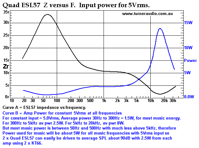
The impedance graph was found published online by about 2003.
My measurements of ESL57
agreed enough to allow myself to re-publish the Z curve but
with added graph for amp power
needed to achieve a constant 5Vrms at speaker terminals.
If you look Z at 100Hz, it is 29r, and power = Vsquared / Z =
25 / 29r = 0.86W, so if sensitivity
was 86dB at 1W, we could say 0.86W makes 85dB SPL. All good
speakers should make the same
SPL for a constant level of Vac applied between 20Hz and
20kHz, which seldom occurs with any
speakers. ESL57 did have a good response graph between about
80Hz and 15kHz.
At 1kHz, Z = 10.5r, and power = 2.38W, and if the SPL remained
at 85dB at 1kHz like,
then 2.38W makes 85dB SPL, so 1W makes about 81dB, so
sensitivity has reduced -4dB.
At 5Vrms there is 6.5W where SPL = 85dB, so sensitivity is
77dB / W.
Quad ESL57 are quoted to have Z = 15r0. But it is only at
280Hz. With 5Vrms giving 85dB
at 280Hz, power = 1.67W, so 1W will make about 83dB. 1W to
15r0 = 3.87Vrms.
Quad-II can make about 16W max for 15r0, with Vrms = 15.5Vrms,
or +/- 22Vpk.
Therefore two Quad-II amps giving 32W could make 98dB, each
speaker is nominal 15r0.
With 2 stacked ESL57 at each channel, and for 64W total, you
get 101dB, speakers are 10r0.
and with 3 stacked ESL at each channel, and for 96W total, you
get 102.5dB, speakers are 5r0.
Quad's original manual says max Vac must not exceed +/- 33Vpk,
or 23Vrms which is 35W for 15r0.
Thus if a high powered amp is voltage limited to +/- 20Vrms,
we might expect ESL57 to remain
intact and not suffer damage caused by arcing panels of too
much Vac is applied. With ESL57,
it is not excessive heating that causes damage, it is
excessive input Vac.
The 20Vrms from 8585 amp is 80W per channel for 5r0 and you
might expect maximum SPL of
105dB for both channels. The sensitivity is perhaps higher
with stacked ESL57, but I don't know
by how much; it could be +3dB at bass F.
Most ppl will not have any idea of anything I just wrote, but
my customer was delighted with the
outcome. It could be expected because the 8585 is well matched
to 3 stacked pairs with each
speaker using less than 1/3 of the power if only 1 pair of
speakers was used.
Amplifier sensitivity is 0.67Vrms for clipping at 80W with
5r0 load.
This is for preamp volume control at max level output using
sine waves. Thus many CD players
which make 1.4Vrms will cause much clipping, but with volume
at 10 o'clock the level will be
just fine.
For common average power levels = 0.8W, Vac at input 1/10
maximum = 0.067Vrms.
In other words, a logarithmic volume attenuator is set to
centre position with 0.67Vrms at input
and SPL levels are not deafening, but comfortable. With a CD
player the volume attenuator may
be set at about 10 o'clock, and if source input is 0.2vrms max
from AM-FM tuner, the volume
control may be turned up to 2 o'clock.
The gain of the preamp was somewhat carefully chosen because
there is no ability to delete
the preamp from the signal path.
In-built line level Preamps.
Each preamp has gain = 2.68 which includes losses for
balance control.
Each preamp has paralleled 12AU7 with active constant
current source MJE350 for Idc with high
Z to anodes. Thus anode load is only 50k volume pot with RLa
for each triode = 100k.
Input levels can be up to 20Vrms before the preamp clips.
If amp input = 1.4Vrms max from a CD player, Max Po from
preamp = 3.8Vrms, and THD < 0.12%.
But at average levels THD < 0.04% = mostly 2H, OK.
See the graph of THD for 8585 input preamp which shows the 2H,
3H, 4H, 5H and 6H as they rise
above the noise floor between 0.4Vrms output and 10Vrms
output.
The 12AU7 preamp has 12dB amount of shunt NFB between its
anode output and grid input to
ensure channel gain remains constant and well balanced and to
reduce THD and noise and Rout.
The input selector switch is a 2 pole x 6 position
silver plated wafer rotary switch supplied by RS
components.
The balance control pot is a cermet type supplied by Farnell,
and the gain control pot is a dual 50k
stereo Alps "Black" carbon track pot which has been used in
numerous quality amps for the last 30
years at least and which is available at RS and Farnell
Components.
Tube Layout
The four front tubes are 12AU7.
The next row of four tubes from the front are EL84 or 6BQ5,
which are exactly the same type of tube,
but with different commonly used type numbers. The rear eight
tubes are the eight matched octal
output tubes.
Fuse Replacement and Home Service
The only fuse which should be replaced by the owner is the 3
amp slow blow mains fuse near the
IEC input mains chassis plug at the rear of the amp. The amp
must have the mains cable removed
from the amp before fuse replacement.
There are other fuses within the amp and placed close to the
appropriate circuit point, and none
should be replaced by the non technically trained owner
without a technician examining why the
the fuse blew. See the list of fuses below the power supply
schematic, Fig 3.
Fig 3. 8585 schematic Power supply.
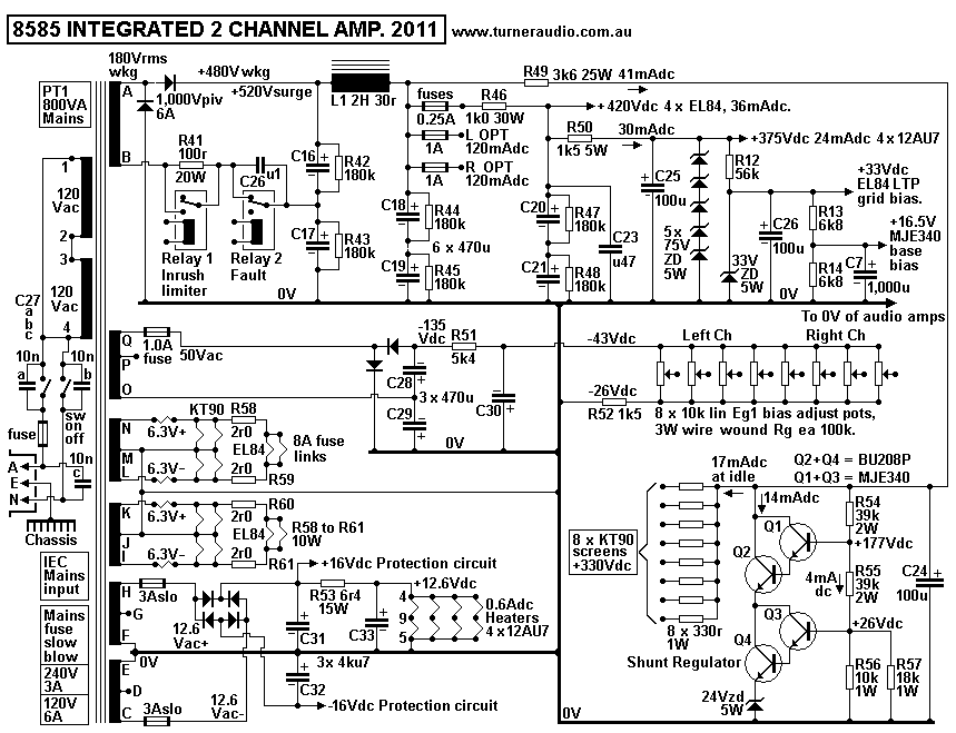
Fuse locations and sizes and mains voltages.
Mains fuse = 3A slow blow, type 3AG, for Mains = 240Vrms, 50Hz
or 60Hz.
Mains fuse = 6A slow blow, type 3AG, for Mains = 120Vrms, 50Hz
or 60Hz.
Changes to Mains voltage settings are done by removing the
central transformer cover.
Mains fuses are externally accessible and mounted in rear
panel.
Anode dc supply fuses, two 1A slow blow, one 0.25A slow blow;
access by removing bottom cover.
Bias supply fuse, one 0.7A or 1A slow blow; access by removing
middle transformer cover
on top of the amp.
Heater filament dc supply, two 3A slow blow; access by
removing middle transformer cover
on top of the amp.
Turn on delay
There is a short turn on delay of a few seconds, only to
prevent excessive input current at the
moment of switch on, and a relay click should be heard 4
seconds after turn on.
Protection
The amp has active protection to prevent one or more of the
output tubes from conducting more
than 3 times the 33 mA of idle current for longer than 4
seconds.
If this ever occurs, a second relay in the power supply will
turn off the main anode dc supply to the
output tubes, leaving the amp turned on with heaters glowing,
but unable to make any sound, but
harmless in this condition. Without any anode current the amp
cannot overheat any part of itself.
During this "fault" condition, the two red LEDs at the front
of the amp will glow to indicate the fault
condition.
Re-setting the amp after tripping the protection during
an accident such as turning up the volume
with shorted speaker leads is achieved by waiting 20 seconds
after turning off the amp and then
turning it back on.
Fig 11 further down this page has the protection
schematic and notes about its exact operation.
The LEDs at the front also indicate the bias condition
of the amp.
When the bias of each output tube is correctly adjusted, the
two LEDs will remain extinguished.
A small variation of bias balance between the two halves of
the PP circuit of each channel will cause
the LEDs to light up.
During normal operation, the red LEDs should remain
extinguished, but during extraordinarily
loud music, LED may flash at times due to some temporary Idc
imbalance. Should noticeable
distortion be heard, and should the LEDs flash at an unusually
low gain setting, something is wrong
with the speakers or leads, ie, they may be shorted together,
or there may be a fault within the amplifier.
Biasing
The amp uses "fixed bias." This is misleading, since if it is
fixed, how come it must be occasionally
adjusted?
Well, once adjusted to the correct level, it remains fixed at
the adjusted level for at least 3 months,
and sometimes for many years without further adjustment being
required. And there are 8 output tubes
which EACH require separate adjustment.
All the 12AU7 and EL84 are automatically biased and need only
be checked during a yearly routine
check up. Output Tube Bias should be checked every 3 months by
a prudent owner!!!
However, owners find that bias adjustment is not needed unless
one or more red LED light up to
indicate some bias drift has occurred.
You will need a voltmeter and flat bladed screw driver with
a thin shaft at least 150mm long.
Bias adjustment can be done without moving the amp from the
equipment stand. Volume MUST
be turned to minimum. Sources and speakers may be disconnected
but usually there is no need.
There are 4 test points on each side of the front panel, with
each test point corresponding to an
adjust screw on the top of the chassis nearby and
corresponding to each output tube, when viewed
left to right.
Each test point is a recessed brass plated philips head screw.
It is safe for an unskilled person to perform the bias
adjustment.
The positive red lead probe of the volt meter is held against
the recessed philips screw head and the
negative black probe is plugged into the hole for the black
lead probe, or simply held against the chassis.
The long flat bladed screw driver is used to reach down
vertically through the mesh tube cover to
turn the shafts of the 8 bias adjustments.
Do NOT turn the recessed philips head screws; these are
not adjustment screws.
The voltmeter is set to a low range of direct voltage, say the
2Vdc range, and is used to measure the
first test point voltage and the adjacent screw on top of the
chassis adjusted in either direction so the test
voltage measures 0.7V dc.
Although slightly awkward, an untrained person may hold the
test leads of the voltmeter with red lead to
the test point, and the other hand can adjust the appropriate
screw.
Make sure that the red lead probe is not shorting the recessed
contact screw to the chassis.
When replacing a tube or all tubes, always check the
bias quickly after turn on and turn adjust screws
to get Vdc less than 0.7Vdc.
Allow the amp to warm its tubes for 5 minutes and then set the
bias of all 8 test points slowly and
accurately to +0.7V dc from points 1 to 8.
After 10 minutes, repeat the bias setting from 1 to 8. As
further heating occurs, the Vdc readings will
change. The adjustment of bias on one or more will affect the
setting of the remainder. After 20 minutes,
repeat the bias adjustment again, and common sense should
allow you to get +0.7Vdc on all bias test
points.
Both the red LED on front panel should remain unlit.
With equal Idc in all tubes, the LED cannot turn
on. If one or both the LED remains alight after the bias
adjustment, you have done it wrong, and turned
the wrong screw whilst measuring the wrong test point, or you
have a problem in the amplifier.
When correct, *all* bias test measure up to 0.7Vdc between
test point and chassis.
The technical reason for +0.7Vdc may not be easily understood,
but here it is :-
The OPT primary has total Rw = 84r. There are 16 layers of
wire with each having average Rw = 5.25r.
Two layers near the centre of bobbin windings are for a CFB
winding which has its CT taken to 0V.
Their average Rw = 5.25r.
There are two x KT88 cathodes plus series 10r0 connected to
each layer of CFB, so if there is +0.7Vdc
at each cathode, the Ikdc flow for both KT88 = 0.7Vdc / [ ( 2
// 10r0 ) + 5.25r ]
= 0.7Vdc / 10.25r = 68.3mAdc.
Therefore Ikdc for each KT88 = 34.15mA. The Ig2 dc = 2mAdc,
and Iadc = 32.5mAdc approx.
The tube Pda = Ea x Iadc = +480V x 0.0325Adc = 15.6W and Pdg2
= 330Vdc x 0.002A = 0.7W,
so total Pda+g2 = 16.3W, and the tubes run cool and will last
far longer than if Pda+g2 was 32W.
The relative rotation position of each adjust screw will be
slightly different with new tubes, and as
the tubes age, the rotation position will vary increasingly.
If it is impossible to obtain enough
adjustment screw rotation to get a +0.7Vdc reading for any
output tube, ie, if Vdc is above or
below 0.7Vdc, it is possible that this tube has a fault,
and it may need replacement.
Overheating?
The output tubes the tubes most likely to ever overheat,
because they are working even when no
signal is present.
If the level used is excessive, or if bias has not been
adjusted properly, or a speaker has a shorted
lead, the idle Ikdc flow may increase, and if Ikdc ever
reaches about 88mAdc, the Pda has reached
the 42W limit for KT88 and 6550.
Each KT88 tube with correct idle Idc may be at about 150C at
the top of the glass. Each output tube
has its cathode heater filament liberating 11.3W, anode may
liberate 25W, screen 3W, so normal total
= 39W. The tube makes the same heat as a 40W incandescent
light bulb at idle, and id Pda+g2 = 45W,
then tube has total heat = 56.3W, and glass will be close to
maximum temperature
An orange glow should be seen at the centre of the box like
structure inside the tube. It should not
be a bright yellow or red, and the glow is the heater element
which is at about 900C. It is a lot cooler
than a light bulb or a tungsten cathode inside 845 or 211
where cathode is at 2,000C+, and appears
white hot. The dark grey outer metal box is the anode
electrode seen easily just inside the glass
envelope. This largest electrode should never appear to glow
red hot itself. If it does glow, T is too
high and there is a fault in the tube operation, and a hand
held above the tube will feel that it is running
hotter than the tubes around it. Usually the bias Vdc at test
point would be well above 0.7Vdc.
But where Vdc goes too high for too long, the protection
circuit usually will turn off the amp before the
anode glows red hot due to excessive Iadc.
Power Consumption
Highest power consumption occurs where the amp works hard to
make a large amount of Class
AB power and where the anode Idc to the 4 output KT88 increase
from say 140mAdc at idle to about
280mAdc. For hi-fi amps this never occurs because there is
never any clipping of music signal peaks
and the average power is often less than 10W. Therefore mains
input power remains fairly constant.
Idle Power consumed for 8585 with KT88 or 6550 or KT90 all set
up the same :-
Output filaments, 8 x 6.3Vac x 1.8A = 91W.
Input 12AU7 filaments, 4 x 12.6Vdc x 0.15A = 8W.
Driver EL84/6BQ5 filaments, 4 x 6.3Vac x 0.8A = 20W.
B+ +Vdc x Idc to KT88 and all others = 510Vdc x 0.36A = 184W.
Bias voltage supply, -132Vdc x 0.020A = 3W.
Sub Total power = 306W. Add PT winding losses of 6% = 325W.
Amplifier is Heavy !
The 8585 needs a sturdy support bench. If it is moved, make
sure all cables are disconnected including
mains cables. The 8585 is 42Kg, and well above the maximum
weight allowed by National Standards for
Unaided Lifting in a workplace. These are about 16Kg in
Australia. After building the 8585 I always made
monobloc amps for where Po max > 50W.
But many heavier tube amps are available from ARC and VAC, and
I like to think my amps give better
music and less smoke per Kg than my competition :-).
I put two large size D handles on each side of amp which
allowed two men to carry the amp more easily.
USE A TROLLEY when carrying the amp from a vehicle to a house.
Never drop a tube amp to a hard surface. The weight of
transformers may deform the steel sheet metal.
Call a friend to help you move the 8585; he will enjoy a
listen afterwards.
As maximum Po rises above 50W, there can be two amp chassis
with only audio circuitry and with power
cabling to a third chassis for Psu for both, or two Psu
chassis, one for each audio amp chassis.
I found that where Po = 300W+ for a single channel the weight
of amp chassis and its Psu each exceed
20Kg.
------------------------------------------------------------------------------------------------------------------------------------------
Output Po and loads
The available undistorted power power varies with load. For
the 8585 the recommended loading for the
frequencies up to 800Hz should average 3r0 or more.
Above 800Hz, the Sec load can reduce, as it does
for ESL speakers. 3 stacked Quad-ESL57 have Z = 5r0 at 280Hz,
and below this the maximum Z is 10r0
approx, which does no harm. But by 2kHz, load reduces to 3r5,
and is 2r7 at 5kHz and 0.6r at 18kHz.
It is impossible for any amp to give the same maximum Po at
18kHz as at 2kHz for 18kHz.
Fortunately, the average level of power for most music
declines rapidly above 2kHz.
Graph 2. 8585 Po vs Sec RL.
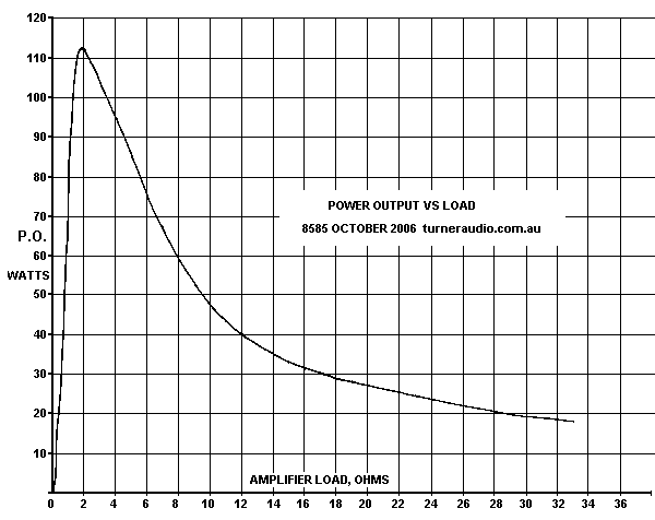
Graph 2 curve shows the power output at less than 1% THD for
loads between 0r0 and 33r0,
4 x KT90 per channel.
Harmonic Distortion products in the 8585 :-
There are 3 following graphs with comments regarding
harmonic distortion production.
Both channels were tested, the results shown are for the right
channel only because curves
for each channel were remarkably similar.
Graph 3. Harmonic THD spectra for 8585, 4 x KT90 per
channel.
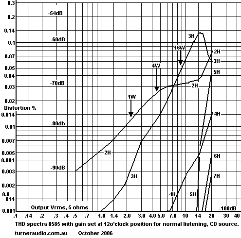
Graph 3 shows the distortion components of 2H to 7H where
relevant, ie, as they increase with output Vac.
There is considerable 2H produced in comparison to the 3H at
below 4W which would cover the average
listening levels of 99% of the population. I think the 2H
comes from slight differences of gm in output
tubes, driver triodes and from SE triodes V1 and V2.
The amount is all less than 0.03%, and at - 72dB, and utterly
negligible. Notice that the dreaded higher
number 4H, 5H, 6H, and 7H harmonics do not appear
significantly until the amp is being worked above
about 37W, ie, at Vo = 13.5Vrms of output, where they try to
rise above the 0.005% level.
Graph 4. Harmonic spectra for 8585 with Vol control at
max
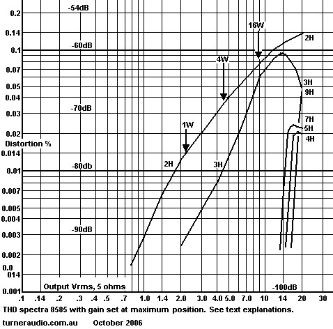
Graph 4 shows the difference in harmonic products produced
when the input preamp has its output
minimized by turning up the volume control to maximum. This
gave less 3H and more 2H especially
at high levels, and Graph 4+4 show the effects of 2H
cancellations when the preamp is used to
produce more voltage before the volume control attenuation.
I first thought perhaps the preamp 2H would add to the power
amp 2H produced in the V2 12AU7
but this appears not to be the case, so the 2H is otherwise
being produced in the power amp.
If output tubes had their positions reversed to opposite side
of PP circuit, perhaps 2H of inputs
would cancel more. So the 2 H measured in PP amps can vary
considerably due to tube placement.
But as you can see 2H at clipping is only 0.14%, and at 4W its
0.036%, negligible.
In PP amps the 3H is usually the most dominant but not under
all circumstances.
In 8585 the 3H is very low compared to many other designs
using such low idle Ia dc levels.
Being able to obtain less than 0.014% of 3H at 4W is a good
result for any tube power amp, and
regardless of the volume control setting. In both Fig 5 and 6,
higher order harmonics are
negligible at ordinary very loud levels.
Graph 5. THD for 8585 for 6550 in 2004, and KT90 2006.
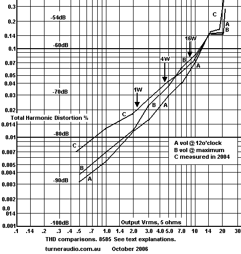
Graph 5 has 3 curves drawn above for THD for the 8585 with
KT90 output tubes. Tubes are biased
lightly with Ia at only 33mA per tube. Curve A and B were
plotted in 2006 after changing from the 2004
schematic for the input preamp. Curve C is derived from the
2004 measurements for 4r0, 6r0, 8r0
in graph 7 below, and for a 5r0 load and with volume control
at maximum to ensure the input preamp
creates the least THD possible.
Curve A is for the 2006 above amp schematic and with
the volume control set at the middle position.
This means that any incoming signal is amplified 2.6 times,
then reduced in level by a factor of
0.156 times by the volume potentiometer.
The curve A was plotted by varying the input signal at 1 kHz
until the amplifier clipped at just over
20Vrms into 5r0.
Curve B was plotted with the same increasing input
signal but with the volume control set to the
maximum level so to reduce the amount of amplification by the
V1 12AU7 preamp and negate its
probable effect on the THD measurements.
Notice that there is a difference between THD levels of
curve A and B and it is due largely to
cancellation effects of the second harmonic distortions
produced in the preamp and power amp.
Curve C is taken from measurements made on the older
schematic presented in 2004.
There is not a huge difference between any of the curves, but
there is a consistent reduction of
THD of at least -6dB between the 2004 and 2006 versions of the
amp, ie, between the curve C and
A respectively. This is mainly due to a reduction of 2H in the
V1 12AU7 preamp by using a CCS
load for the anodes and due to 12dB of shunt NFB to reduce the
12AU7 gain.
The older 2004 preamp relied only upon about 4dB of current
NFB from the non bypassed 1.5k
cathode R of the V1 12AU7.
At low levels the reduction in distortion due to a large
increase in NFB does not result in an exactly
proportionate THD reduction when the preamp is tested with the
power amp.
Graph 6. THD of SE 12AU7 preamp in 8585, 2006.
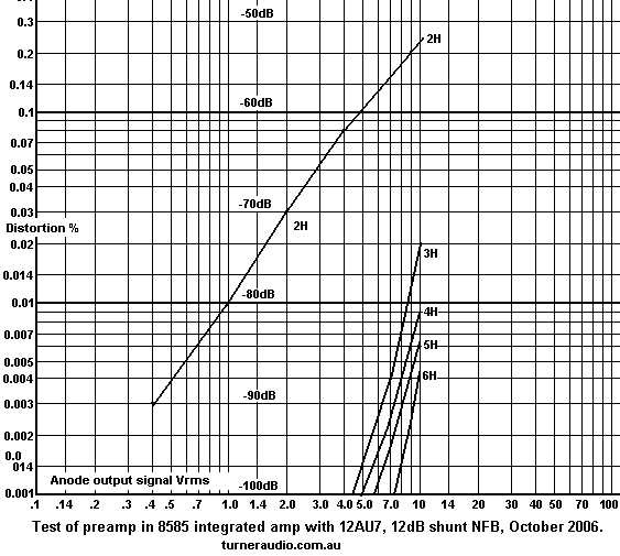
Graph 6 shows the THD result for the V1 12AU7 triode line
level preamp built into the 8585.
I measured the harmonics up to 10Vrms output only because when
testing high output resistance
circuits above 600r my test gear has to use a high input
impedance low distortion buffer between
the device under test and the analyser whose maximum input Vac
limited to 10Vrms.
There is no point in measuring output voltages above
10Vrms because it is extremely unlikely
the input preamp would ever have to produce more than this
voltage level. It is of course capable
of about 60Vrms of output. As can be seen the THD at 2.6 Vrms
of anode output which would be
due to a high level input from a CD player, THD = 0.04%,
mainly 2H with ALL other harmonics
below the noise floor.
People forget just how linear triodes can be.
There are those who despise and discourage the use of NFB to
reduce noise, output
resistance and distortion on the grounds that a small amount
of it such as I have used
around this preamp will significantly raise the higher order
harmonic products above the
2H to become a serious sonic pest. There is NO evidence that
they are correct.
I am convinced that 3H or other harmonics all at below the
0.001% level do not have
any effect on the sound quality at all.
-----------------------------------------------------------------------------------------------
Graph 7. THD for 8585 measured in 2004, 4r0 t0 8r0.
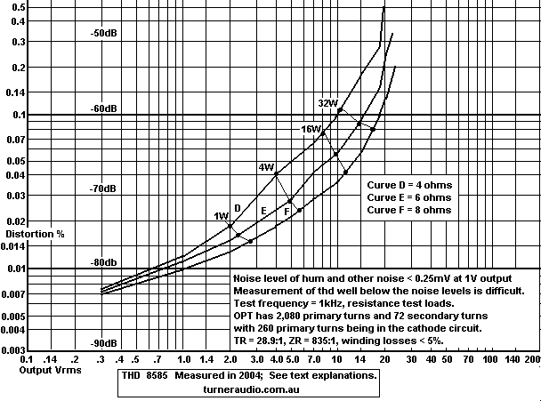
Fig 10 is the THD measured in 2004 with the 2004 schematic of
Fig 8 below.
Notice that even without the improvements to the input preamp
section of the amp the THD
is below 0.1% for any load above 4r0 and any power below 30W.
The further analysis of
the THD spectra in 2006 shows that there are very small and
insignificant amounts of high
numbered harmonic content above 3H.
The THD measurements were taken with Ia = 40mA at idle per
each output tube.
Should the bias Iadc be increased to 60mA, the THD into 4r0
which is the worst would be
reduced from 0.04% at 4W to 0.03%, a negligible improvement.
The best fidelity is gained with loads above 4r0. The THD
reduction with more idle Iadc for
more class A would not be audible, and not worth the cost of
wearing out the tubes sooner,
and dissipating an extra 76W of heat within the amplifier. The
2006 version of the amp
has better measurements than those in 2004 even though 2006
amps makes less initial
class A Po.
Notes about Push Pull Distortion
Push Pull amps have inherently low distortion even without any
use of NFB at all, providing
the tubes work in class A.
If one imagines two men sawing a log with a long bush
saw, with each man at each end of
the saw. ( This is how much timber sawing was done before
chain saws etc. )
The motion of the saw is fairly smooth and regular with one
man pulling, and the other pushing
the saw, and the individual motional irregularities of one man
is cancelled by the other man's
similar irregularities. If you used a computer to record the
motion of the saw over time, a wave
form could be produced, and the distortion would be found to
be less than if both men worked
at just one end of the saw.
Similarly, using two Push Pull tubes avoids the higher
distortion of using the same two tubes
in parallel to produce the same power for load R.
Power, P, in watts, = V x I, liberated as heat in a
load R.
This is part of Ohm's Law where R = V / I.
Thus V = R x I, or , I = V / R.
Thus it is equally valid to say P = R x I squared, or
, P = V squared / R. These formulas MUST
be riveted to the brain of anyone attempting to design the
simplest amplifier.
The two men at each end of saw both produce the same motion
shape if you saw a graph, and
each produces a similar amount of power ( if they have nearly
matching physiology characteristics ).
But the TIMING of each man's wave motion is oppositely phased,
like their two children in a
see-saw where one is up high, the other is low near the ground
and at some point they are at
equal height, but moving in opposite directions.
Each man and each child produce the same power power as their
companion.
The push power or one man sums with the pull power of the
other to make an average force
to move the saw that is nearly equal for both directions, and
lasts for the same time.
In a PP amp with 2 x KT88 at each end of a primary push-pull
winding, when current increases
in one tube it decreases in the other tube. The power
liberated = V change x I change.
The principle of PP action has been used since about
1910, and it confuses all non technical
people although two kids on a see-saw are using the principles
of push pull action without
knowing what it is, at least until they grow up and study
physics.
Before 1910, many early amps were SE, "single ended", where
one tube worked alone like
one man with a saw. ( but you cannot have an SE see-saw ).
A single tube can be used for audio for class A operation
using adequate amount of NFB.
Many ppl prefer the music with SE amplifiers, but my
experience proved to me PP or SE
could both deliver the finest audio quality possible.
The idea of linear analog amplifiers has been with us
since before 1910, but is now being rapidly
replaced by amps using Pulse Width Modulation where the bjts
or mosfets used in power amps
do not need to be linear, but must only need to turn on and
turn off fast for a square wave at say
200kHz. The wave time for 200kHz = 5uS, and the rise and fall
times should be a tiny fraction
of this, say 0.25uS, and if the Psu has a 50Vdc rail, the rise
+ fall time = 50V per 0.25uS, or
200V/uS, something that not all tubes are suitable for.
PWM is explained basically at
https://www.youtube.com/watch?v=YmPziPfaByw
The bloke explaining how easy it is to control motor speeds or
LED brightness. load V change
could control a speaker cone if the signal output devices with
PWM output signal have an L+C
low pass filter to prevent the HF switching noise appearing at
the speaker.
The difference in analog amps and PWM amps is that the analog
devices dissipate heat while
generating audio power, but the PWM devices spend more than
95% of their time either switched
on with P = 0V x I or off with P = 50V x 0.0 I, so there's no
heat in devices and the load V and I
is the average, and power is not wasted in amp devices so a
600W 6+1 home theatre amp is
a lightweight box that never gets hot and costs less to make
than a 100W stereo amp from 1980.
But don't throw away your tube amps. You may find you like the
sound better than any PWM amp.
In most tube power amps the THD is mainly due to output tubes
with maybe 25% due to input
and driver stages which don't have to work as hard at output
tubes. THD need be reduced to
below 0.05% for average levels and any further reduction is
difficult for anyone to detect.
Protection circuit.
Fig 4. 8585 active protection for 8 x output tubes.
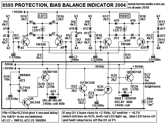
Fig 4 shows the schematic on a circuit board under the chassis
about 150mm x 100mm.
The schematic uses easily obtainable discrete bjts, diodes,
LED, and one SCR.
Notice the absence of op-amps which I humbly suggest should
never be used in any tube
amp for any reason. The schematic encourages the tubes to
remain well behaved while parts
around them mail fail, or while an owner's teenage son tries
desperately to see if roof tiles
will rattle with gross overload. Here I use bjts to be slaves
to protect the tubes.
Thus there should never be a plume of smoke and terrible sound
during a dinner party.
Partially delayed turn on.
When the + / - 16Vdc rails are quickly established a second
after turn on, idc flows in R19 15k
to charge up C5 470uF and the time constant is 7 seconds for
C5 to reach about +10Vdc.
But while Vdc rises, 8.2Vzd conducts some current before 7
seconds Q5 is turned on.
This makes current flow in R20 2k2 so Q6 BD140 turns on and
Delay Relay shunts R41 100r
20W in Fig 3 PSU schematic. Thus R15, C5, Q5+Q6 and relay and
R41 give a 4 second delay
before R41 in shunted.
After turn on, there is a large surge of primary input due to
all B+ caps being charged up plus
some higher Iac in cold filament heaters for cathodes while
their resistance is 1/2 that when hot.
The highest input current is due to charging B+ caps, and R41
100r much reduces the peak
currents during the first 4 seconds and B+ slowly reaches
about 70% of max in 4 seconds and
then R41 is shunted and a second surge of input Iac occurs
which brings B+ up to maximum.
This allows a mains fuse that is 1/2 the value it would
otherwise be. If the mains fuse was twice
what I show, the fuse would only ever blow AFTER some fault
had damaged something in the
amp. You want the mains fuse to not be useless while something
burns.
Protection.
Filtered Vdc signals from each output tube cathode of L and R
channels are fed to a pair of
differential amps to indicate Idc balance in output stage and
if a fault occurs.
Consider Left channel.
The Vac and Vdc from cathodes k1+k2 each have R1+R2 4k7 +
d1+d2 to feed R3 4k7 and Q1
base. d1+d2 allow only the highest Vdc at k1 or k2 to get to
Q1 base, and where Vac at k1 and k2
increases during normal use to about 37Vrms maximum, the
average Vdc at k1+k2 will rise above
the idle level during class AB operation. The 4k7 with series
diode will cause some some rectifying
of the Vac to increase the Vdc at C1, but the Vdc rise is
slight. C1 100uF shunts nearly all Vac so
Q1 base reacts to average Vdc levels from k1+k2. d1 and d2
form a simple logic circuit so the
higher k1 or k2 Vdc appears at Q1 base.
The same thing happens with k3+k4 and Q2 base, and during
operation, the Vdc at C1 and C2
and two bases remains remarkably equal unless one of more
tubes conducts too much Iadc.
The collector Idc for Q1+Q2 is normally close to equal despite
the high differential gain of Q1+Q2.
Thus Vc of both remain about equal so that no current flows in
d4,d5,d6,d7, and LED 1 remains
unlit. But if the Idc balance becomes a few mAdc unequal,
there is a difference in Vb, and it is
amplified at collectors, and the LED1 turns on. It does not
matter which tube of 4 conducts too
much Idc, it turns on LED 1 to let the owner know he may have
a bias problem. The same thing
happens if one or more output tubes conducts less Idc than
normal.
During high Po production in class AB, the BALANCE of Idc
remains remarkably equal and LED1
remain unlit while tubes are very busy - unless there is a
tube / bias problem.
Both left and right channels have their single LED to indicate
bias balance status.
To ensure the Led remains unlit at idle, each tube must be
biased for equal Ikdc, ie, +0.7Vdc
at each test point for each output tube.
All 4 bases of the Q1-4 have diodes to a common point at input
of R22 2k2 to base of Q7 emitter
follower. The diodes don't allow the bases to ever connect to
each other. If one of the four bases
reach about +2.1Vdc, Q7 emitter will follow the rise to
produce about 0.8Vdc at input of R24, so
Vdc at C6 100uF will rise.
If the +Vdc at C6 increases to +0.68Vdc and gate input current
reaches 30uA, the SCR turns on,
and stays turned. The SCR turns on both LED1+2 via d8+d19, and
turns on Fault Relay which
turns off HT winding on PT1, and blue "on" LED is turned off.
The music stops. Turning the amp
off, waiting 20 seconds, then back on resets the amp plus
protection circuit for normal operation
but if the problem with caused the SCR to trip remains, amp
will stop working.
The amp only turns off due to excessive Idc in any one or more
output tubes.
--------------------------------------------------------------------------------------------
Negative Feedback explained, NFB
Negative feedback occurs in many systems employed by men and
women in their daily lives.
There is even NFB used in principle in your toilet. Every time
you flush the loo, the water empties
from the small tank (aka cistern) on the wall, and water flows
in plumbing pipes and cistern tank
is re-filled. There is a float in the tank which sends a
message via a lever to a valve controlling
the water flow so that when water raises the float, the
control valve shuts down the water flow
and tank remains full without overflowing onto the floor, and
the process is automatic and you
don't need to open a tap and shut it each time you use the
toilet. There is nothing negative about
this positively pleasing fact about our toilets. The flushing
toilet arrived after plumbing found its
way into houses probably at the time your great great
grandmother complained about the stink
and cost of servants to deal with your great great
grandfather's horrible toilet habits, especially
after eating curry, and downing too much ale.
When the full tank evaporates some water, level drops, valve
slightly turns on and level remains
full. It works as well as a good regulated +Vdc supply.
Thermostats for air-conditioning work in the
same way; a temperature sensitive device causes air con to
turn on when its hot, or heating to turn
on when its cold, we don't need to pay servants to haul wood
for fires or to hire a punkawallah to
work a fan to cool us in weather.
The message from float lever or thermostat is called negative
feedback, because the message
opposes the unwanted action of input message; the tank valve
stops water overflow. And if the
water pressure in plumbing doubled, the water level in the
tank may only rise very slightly.
If you have let your front yard look like a mess with old cars
and "stuff" laying about with long grass,
you may get a message from your missus, "Oi, tidy up or
else..." if you fail to respond, She Who
Must Be Obeyed may try more drastic measures to enforce
tidiness. If you tidy up, she calms
down, and the negative feedback has restored domestic bliss
with low distortion and less
intermedulation.
Fig 5. 8585 basic shunt NFB in preamp.
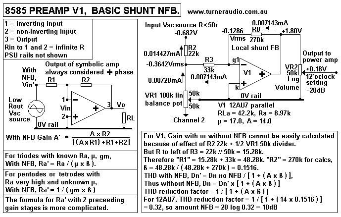
Fig 5 shows the basic operation of shunt NFB. There are
numerous forms of feedback, FB,
and they are series voltage NFB, series current FB, shunt NFB,
as in Fig 12, and a few forms of
voltage and current positive FB which has its uses, but not in
audio amplifiers.
The Left Side diagram of Fig 5 shows a basic drawing
amp to give output Vac between
output terminal 3 and 0V.
There are two inputs 1 and 2 with 2 to 0V and 1 as the input
terminal which is inverting, ie, if
gain = 14, then +1V at input 1 produces -14V at output 3.
The gain A is always considered constant for fixed RL. If gain
A = 14, it is typical of a parallel 12AU7
with a total anode load of about 42k.
The Vac input is from voltage generator with low Rout at least
1/100 of the value for R1.
R1 and R2 form a resistance divider between Vac source and amp
output. It is assumed input 1
is a grid of a tube or very high input resistance at least 100
times R1.
The low Rout for source and high Rin for input 1 enable the
equations for gain and NFB to be correct.
The formula for gain with NFB is different to those used in
text books for op-amps which have typical
open loop gain A = 50,000. This formula here works for devices
with low A such as a 12AU7.
ß must be understood, and it is the fraction of the
output signal that MUST always try to appear
at input.
ß = R1 / ( R1 + R2 )
With no source Vac, if some external factor causes Vo change
of say -1V, the V change at input 1
= -1V x ß and this will in fact try to produce an output Vo
that moves + to oppose the forced change
Vo by -1V. So R1+R2 enable a NFB effect.
Without NFB, the output resistance of a 12AU7 might be 9k0,
but with R1 = 48k and R2 = 270k,
the Rout will reduce to about 2k5, and the bandwidth of 12AU7
is much increased.
While an input -Vac is producing a +Vac at output, there will
always be some distortion, Dn, at
output because no device is perfectly linear.
Distortion without NFB = Dn, and with NFB it is Dn'.
With R1 = 48k and R2 = 270k, ß = 48 / ( 48+270 ) = 0.1509.
If +Dn' appears at output with NFB, then +0.1509Dn appears at
input 1 and the inverting gain of
14 produces output Dn = -2.1126Dn, and this is niether Dn' or
Dn, but is called the Error Correction
signal, which might be labelled EC.
To most people, this is utter nonsense, because if you measure
+Dn' at output with NFB, it has +phase,
so is +Dn', yet I will tell them -2.1126Dn does exist at
output, and they still refuse to believe me, so
I tell them the -2.1126Dn is the error correction, and that EC
subtracts from the +Dn that would have
existed before NFB was applied, and +Dn' = +Dn - EC.
Thus +Dn' = +Dn - ( -2.1126Dn ) = +3.1126Dn. So the NFB
reduces +3.1126Dn to +1Dn.
In other words, where Dn' is measured, Dn without NFB =
Dn' x [ 1 + ( A x ß ) ].
If Dn is known without NFB is applied, Dn' with NFB = Dn /
[ 1 + ( A x ß ) ]
if you measured Dn' = 0.1% at output with NFB, then Dn without
NFB = 0.31126%.
The THD reduction factor = Dn' / Dn = 0.1% / 0.31126% =
0.32127.
The amount of NFB applied in dB = 20 x log of THD reduction
factor = -10dB approx in this case.
All this NFB behavior is correct for where the load RL for amp
remains constant with or without NFB,
and the device works in class A and Vo level is well below
clipping.
The diagram on RIGHT side Fig 5 shows a simple amp
representing 12AU7 as it is for V1 in 8585.
In the diagram there is a divider R2 22k plus 50k of 1/2 100k
balance pot. If the input signal is from a
Vac source with low Rout, then input Iac in 22k must be the
sum of Iac in 50k and 33k.
I show the various Vac and Iac for V1 12AU7 which has A = 14.
regardless of all shown Vac and Iac for signal, the R1+R2
divider does exist with regard to THD.
So what is R1? it is the effective R looking to left of grid
input.
With low Vac source at input, 22k + 50k are in parallel to
left of 33k, so are 15k approx, so total R
which form R1 = 15k + 33k = 48k. R2 = 270k, and no other R are
involved.
Therefore ß = 48 / ( 48+270 ) = 0.1509 approx, and the Fig 12
explains what is happening.
It would be possible to make a complete formula to cope with
presence of 22k + 50k but I see no
reason, and ability with mathematics may add the needed
formula "which includes all possible
deviations from Simple" But I know that adding 33k + 270k
would give an approximate reduction
of THD by -10dB and reduce the gain of V1 which still leave
enough gain for convenient operation
of amp with input Vac between a nominal 0.2Vrms to 2Vrms. The
270k does not much reduce RLa for
12AU7, and the 33k does not upset the input Vac path, or make
amp input Rin too low.
The shunt NFB always does reduce amp input R. In 8585, it
could never be less than 22k which is
quite OK for any CD player of digital Vac source.
The model works works for a pentode such as 6BX6 with same
Idle conditions of 12AU7.
But the pentode Ra without NFB may be so high, 500k+, and is
difficult to measure, and so is gm
and µ. But where Ra is known to be more than 10 x RLa, the
approximate gain A = gm x RLa
so gm = A / RLa, and for 6BX6 in 8585 for V1, A might be 168,
and if RLa = 42k, then gm =
4mA/V. With shunt NFB, Ra' = 1 ( gmg1 x ß ). With same R1 and
R2 shown,
Ra' = 1 ( 0.004A/V x 0.1509 ) = 1.656r, so the NFB makes a
very big difference to Ra.
If Dn was say 0.321126%, same as 12AU7 at same Vo without NFB,
then
Dn' = 0.31126% / [ 1 x ( 168 x 0.1509 ) ] = 0.0118%, much less
than 12AU7 with 0.1%.
But usually 6BX6 would have 3 times Dn without NFB than 12AU7,
so the Dn' with NFB is only
marginally less for 6BX6, and contain more H spectra. 6BX6 is
not made now, so use of triodes
is more practical and does not need a B+ screen supply. If you
wanted less THD than 12AU7,
you could use parallel 12AT7 with A = 40, and Dn = 0.044%
Fig 5 may produce understanding after several days of study.
Many ppl just cannot understand,
or they say they cannot accept any form of NFB, and they
expect devices to be distortion free,
but not one device is ever perfect.
Fig 6. 8585 basic GNFB in power amp.
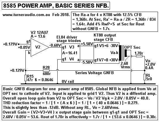
The power amp within the 8585 has V2 parallel 12AU7 SE
triode as a differential amp with one
anode output driving V3+V4 with two EL84 in triode mode
arranged as long tail pair differential amp
with balanced outputs from 2 anodes. The EL84 drive the grids
of V5+6+7+8 KT88 which drive an
OPT with ZR = 834.
The simple model shows overall gain between V2 Vg-k and OPT
sec = 40.0. Vac levels are at 1/10
clipping levels. All output tubes work in pure class A to make
0.8W for RL = 5r0, and this level will
give levels that are quite loud with average sensitivity
speakers.
Beta, ß = 47r / ( 680r + 47r ) = 0.0646.
I show how the "-12dB GNFB" reduces THD by factor = 0.279
which is really about -11dB GNFB.
Notice that the amount of GNFB reduces with lower output RL
because Gain A is reduced. But with
no load at all, gain A = 53.6 and THD reduction factor = 1 / [
1 + ( 53.6 x 0.0646 ) ] = 0.224, so
maximum possible amount of NFB applied is about -13dB GNFB.
Most error correction occurs in output stage so the input and
driver stages do not have to generate
a high error signal so they do not produce much
intermodulation.
The GNFB in power amps increases the bandwidth found without
any GNFB. The input+driver stages
contain R+C networks to shelve the open loop gain at very low
F and very high F outside the AF band
of 20Hz to 20kHz. There are Zobel R+C across each 1/2 primary
and across output to load the output
stage at HF where loudspeakers may have no loading effect
above 25kHz. There is a 680pF across
680r GNFB R which begins to advance the phase of Vo fed back
at above 100Hz.
--------------------------------------------------------------------------------------------------------------------
Graph 8. Loadline analysis for 4 x KT90 PP with 12.5% CFB.
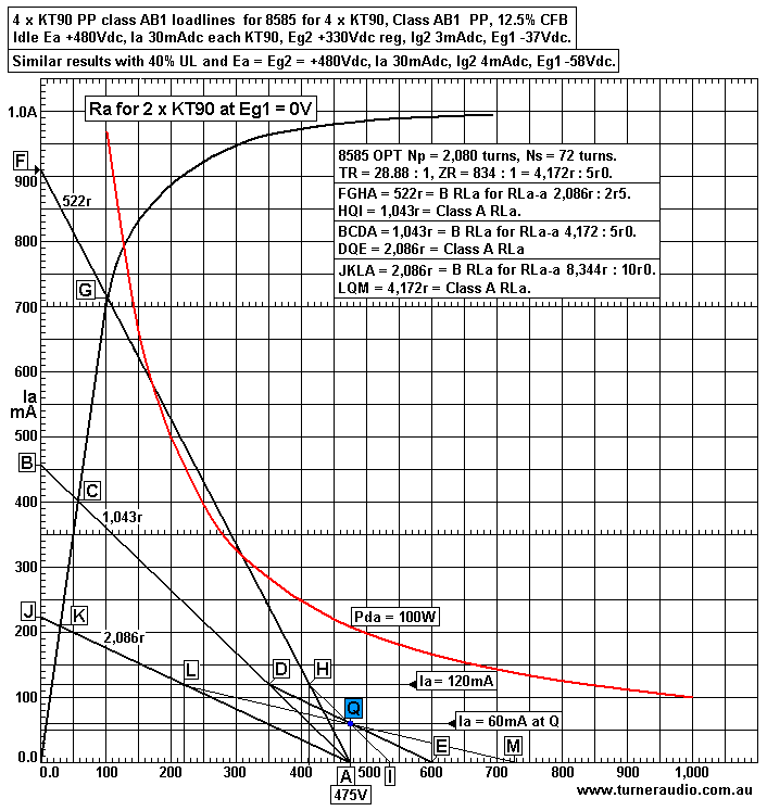
Graph 8 is not a determined attempt to confuse everyone, but
you *will need* to think about what it
all means!
I suggest those who don't understand load line analysis should
read the basics in the Radiotron
Designer's Handbook, 4th Ed, 1955, or my other pages on load
matching to PP tubes.
Above, the 8585 amp is described and has an OPT with load
match ratio, aka impedance ratio,
aka ZR = 4,172r : 5r0, to suit 4 x KT90 arranged to power 3
parallel stacked pairs of Quad ESL57.
The load lines for the 8585 load as specified may be plotted
as follows :-
1. Draw up the combined Ra curve for TWO KT90 in parallel.
This is shown as a curve from 0.0 thru
K, C G and swinging over to the right below Ia = 1,000mA. This
curve is generated by doubling the Ia
change for a given Ea change along the Ra curve for Eg = 0V
shown in data sheets for ONE KT90.
The KT90EH I have used is very similar to KT88EH and 6550EH
and old original 6550 and KT88.
2. Draw the Pda limit curve for 84W, which is twice the
maximum allowed Pda for KT88 and 6550.
The 8585 is able to use 6550, KT88 or KT90, so the load lines
above are valid for all 3 tube types,
as well as the more recent EH KT120.
3. Plot Point Q at Ea = +475V and Ia = 60mA. This is the
Quiescent idle point for 2 x KT90 on each
side of the PP circuit.
4. Calculate the B RLa which is the Class B load when the
operation has moved above the Class A1
to AB1 threshold.
B RLa = 4,172 / 4 = 1,043r.
5. Plot Point A vertically below Point Q on Ea axis.
6. Calculated Ea / RL B = 475V / 1,043ohms = 455mA.
7. Plot Point B on Ia axis at Ia = 455mA.
8. Draw line from B to A. This is the loadline for 1,043r.
9. Plot Point C where Line B to A intersects the Ra curve for
Eg = 0V.
10. Plot Point D on Line B to A where Ia = twice idle current
= 120mA.
11. Read off the Ea vertically below Point C = +110V. This is
the point which sets the limit for Ea load
swing with this RL, and is E min for the load voltage swing.
12. Calculate Peak Load voltage swing for RLa-a = 4,172r. Peak
load voltage for RLa-a
= 2 x ( Ea - Ea min ) = 2 x ( 475 - 110 ) = 730Vpk.
Calculate Va-a in Vrms = 730 x 0.707 = 516.11Vrms.
13. Calculate maximum output AB1 power = Va-a squared / RLa-a
= 516 x 516 / 4,172 = 63.8W.
14. Read off the Ea vertically below Point D = +350V.
This is the voltage point where the class A1 operation ceases,
and class AB1 begins.
Calculate ( Ea at Q ) - ( Ea at Point D ) = 475 - 350 = 125V.
Add this to Ea at Q, 475 + 125 = 600V.
Plot Point E on Ea axis at 600V.
15. Draw straight line from D thru Q and it should proceed
thru Point E at 600V.
Line DQE is the load line for the class A portion of power
produced by 2 x KT90, and is equal to a
load of 2,086r. Each pair of KT90 on each side of the PP
circuit have the same Class A and AB loading.
The voltage between Point D and E is the peak to peak load
voltage for class A for 2 x KT90.
16. Calculate Class A portion of power for 4 x KT90.
Peak to peak voltage for 2 x KT90 = 2 x 125V = 250V.
Va rms for 2 x KT90 = 250pk-pk / 2.82 = 88.65Vrms.
PO for class A RL a, 2 x K90 = Va squared / RLa = 88.65V x
88.65V / 2,086r = 3.77W.
Class A portion of PO = 2 x 3.77W = 7.54W.
Summary so far :-
For 8585 in this case, nominal output RL = 1/3 of of the
nominal 15r0 for 1 Quad ESL57.
The ESL57 was designed to be used with Quad-II amp with 2 x
KT66 produced before the ESL57
was marketed.
The Quad-II amp gave about 22Wb to 15r0. Therefore an amp
capable of 66W into 5r0 should be
capable of adequately powering 3 parallel ESL57. When the ESL
are paralleled and stacked one
above the other, the sensitivity increases perhaps +3dB. So
the same power used for one ESL57
should give higher SPL with 3 stacked ESL. But Quad-II does
not have an OPT allowing a good
load match to 5r0. The 8585 described here will drive the
stacked ESL with ease.
The original Quad-II amps relied on their pure class A ability
to provide fidelity. Their power supplies
are quite inadequate by today's expectations. When the Quad-II
OPT is strapped for 15r0,
the RLa-a is about 4k0, and the extent of class A power = 9W
approx, with an additional 13W in class
AB1. But ESL57 has Z shelf at 10r5 where tube load = 2k7, and
class A = 6W, and class AB is less.
At higher F the Z reduces further and amp will become muddled
sounding with high levels of sound
above 5kHz. Most ppl in UK found Quad-II sounded fine because
they rarely used more than 0.5W
in their small rooms.
Graph 8 has load lines for RLa-a = 2,086r : 2r5 and also
8,344r : 10r0. These load lines may be drawn
using a similar steps of 1 to 16.
Picture 2. 8585 view of under-chassis space filled with
parts.
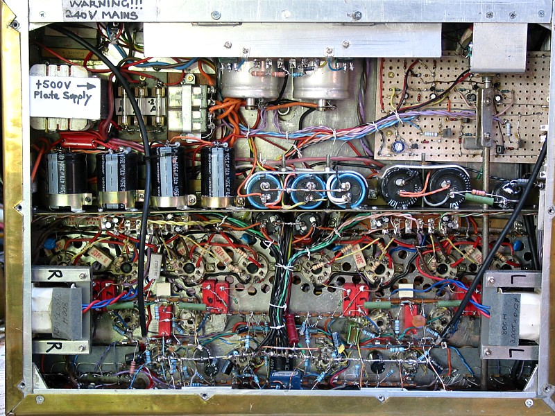
Picture 2 is 8585 in October 2011, view under the chassis,
after a full service following 6 years
of trouble free operation, even though the owner said he uses
the amp daily.
All KT90EH tested similarly to brand new tubes, and showed no
signs of wear, ie, gassiness,
cloudy gettering, or positive grid current at idle. All input
and driver tubes measured perfectly,
and gave no noise. The servicing was required because four
zener diodes I had used had
degraded to having much less than their rated zener voltage of
75Vdc, so the shunt regulator
for the KT90 screen supply produced Eg2 = 200V instead of
+330Vdc, and this turned off Iadc
in all KT90.
I have replaced the simple 4 x series zener diodes with the
BJT based shunt regulator mounted
on the AL angle flange seen at the top of the picture.
Unfortunately, even though zener diodes
may be rated for 5W, they can fail if subjected to only 1.5W
of heat production, and in practice it
is wise to never let their Pd rise above 1/10 of their
official rating.
Other zener diodes in the 8585 have been retained since they
were originally installed in 1996,
and they show no sign of change.
The point to point circuitry is somewhat messy, but quite
reliable, and it is easy to figure out where
parts shown on the schematics are located.
Amplifiers I have made in recent years are a lot neater under
the chassis, Nobody can be as
neat as a well done printed circuit board. Unfortunately, the
use of printed circuit boards obstructs
the flow of air up and around the parts and up through the
holes drilled in the top plate of the amp
and past the glass of the output tubes.
If one looks into the finest samples of circuit production
used in professional test equipment as
manufactured by Tektronix, or Lavoie, you will find 3
dimensional pint to point circuitry, and neatly
bundled wire looms of multi coloured wiring, with much thought
and design given to the location
and placement of each item to maximize component density, yet
disallow adverse stray signal
coupling, and to minimize operating temperatures of
everything.
-------------------------------------------------------------------------------------------------------------------------------
Fig 7. OPT-4B 100W PP CFB / UL for 4k0 : 1r9, 3r3, 7r5.
All the OPT details are shown with the bobbin winding layer
details so that all good coil winding
trades persons will be able to wind a bobbin for you.
The original OPT used in 8585 in 1996 had the same E+I core
size, T44mm x S62mm as above.
But I used NOSS E+I core material with max µ = 3,500, and Bac
max 1.3T. Although LF distortion
with NOSS is slightly higher than GOSS I recommend above, in
practice it made ZERO difference
to the sound because such a large core was used, and Bac is
low even at high music levels.
This design for 2018 has the same 2,080 Primary turns using
0.4mm Cu dia wire. The original 8585
interleaving pattern had 5S + 4P sections and only 2 Sec load
selections. But the above has 4S + 5P
sections to give the same wide OPT bandwidth but has 3 load
matches for any speaker above 2r0.
This OPT could be used for 4 x 6550, KT88, KT90. 4 x KT120
could be used with higher B+ at say
+600Vdc, and max Va-a for 4k0 could be 757Vrms for Po = 135W,
allowing for winding losses.
Fsat is slightly higher at 19Hz. All amps I have ever tested
which had Fsat < 20Hz at full rated Po
gave excellent bass performance.
For those who never need more than 50W per channel, ( about
98% of the population ) they should
link the Secs for 3 parallel windings each 60t comprising
45t+15t in series, for Nominal load ratio
= 4k0 : 3r3. The 3r3 suits the dips in 4r0 speaker Z, and if
8r0 speaker is used, max Po = 50W and
initial class A could be 22W, with all 4 tubes having idle Pda
25W with Ia = 47mAdc.
I found the idle Pda levels for 6550, KT88 and KT90 could be
only 16W, with Iadc in each at 33mAdc,
and yet there is still enough initial class A and flawless
music. With the low idle Pda of only 16W,
I found EH KT90 lasted much than if Idle Ia was 50mAdc for Pda
24W.
Some manufacturers have 6550 or KT88 with idle Pda at 30W. The
original 8585 has B+ at +400V
and Ia = 60mAdc, ie, 24W each. I used 8 x GE6550A NOS which
certainly sounded fabulous, but they
all wore out in 6 years. I have found the EH Russian KT90
tested like new with lower Pda after 6 years.
The 8 output tubes in a row and close together do not become
hot with low idle Pda, and holes in chassis
around sockets to allow air flow.
Without the heat stress, there is only the music to behold.
For more ideas on load matching and how tubes work go to my
list of educational and DIY pages.
---------------------------------------------------------------------------------------------------------------------------------------
The older 8585 schematic from 2004 is included here
for reference.
R+C Part numbers have no similarity to numbers used in above
schematics.
Fig 8. 8585 schematic 2004 for input and power amp.
The schematic was hand drawn before I had time to spend doing
it properly with MSPaint,
Windows XP version.
To Index Page