SOLID STATE AMPLIFIERS 1, MOSFETS.
The contents of this page include :-
Brief note about my experience with solid state amps,
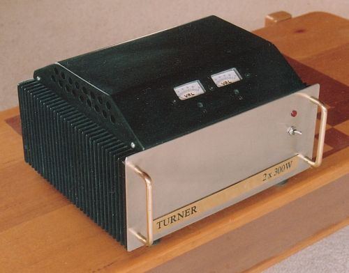
Picture of 2x300W amp.
Schematic of 300W AB amp channel with mosfets.
Schematic operation, topology, heatsinks, performance
specification,
NFB, thd, output current limiting, input voltage limiting, class A
operation.
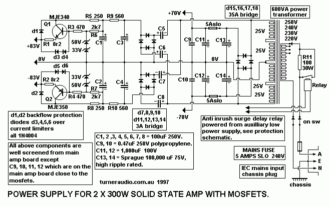
Schematic of 600VA power supply for stereo 2 x 300W amp.
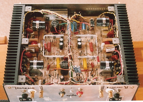
Picture of amp underside.
------------------------------------------------------------------------------------------
Although I try to specialize in tube amps, I have not always
avoided building
fine solid state amps and repairing them.
In 1993 I became seriously interested in all audio hi-fi
amplifiers at a time
when I thought I should change trades from construction work to
something
else.
My first project was upgrading a solid state Linear Design am/fm
receiver
I had bought in 1977 after I had forgotten how fine tube
amplifiers could be.
But later in 1993, I thought I should build a "better" dedicated
stereo amp.
I used two 100W mono amp kits designed by David Tilbrook who had
his
design published in ETI magazine in the 1980s. These kits were
available
in 1993 from a Jaycar outlet which had just set up a Canberra
store.
I very quickly learnt that the output mosfets and the input driver
transistors
were far easier to destroy than tubes by careless workshop
practices and
accidental short circuits.
After fusing a few transistors and mosfets I learnt to be very
careful with
everything I did. Direct coupled solid state amps with many PCB
tracks
close to each other are very prone to instant smoke with a
careless short
somewhere such as a splosh of solder, or from soldering two points
which are not meant to be soldered, or from tiny wire offcuts and
junk
sitting on soldered up boards. The speed of transistor failure is
that of
greased lightning, and unlike tube amp stages there is no R&C
coupling
which allows each stage to be more easily measured before anything
overheats to badly.
That first SS amp had 2 cascaded differential input stages instead
of just one.
Both used BF469/BF470 video transistors. The mosfet output stage
was in
source follower mode.
It was very easy to get excellent thd measurements, and the
circuit open loop
gain was so high that it could not be tested without the global
NFB connected.
It tended to be unstable above the AF band and in 1993 I was not
well skilled
about critical damping stabilization networks around a gain loop
where open
loop gain was extremely high which meant the amount of applied
global NFB
was also high.
The sound was no better than the sound I had enjoyed from my all
bjt Linear
Design receiver.
Following these efforts I read all the Wireless World and
Electronics World
magazine articles on audio from 1917 onwards.
The local Australian National University had all the old
magazines in their
basement archives.
Mr Tilbrook's design was abandoned because the second differential
gain stage
was simply not required to get thd and Rout low enough, ie, below
0.01% at
just under clipping, and Rout less than 0.05r. If the THD = 0.005%
at 100W,
then at 2W the THD was difficult to measure, ie, inaudible for
levels
used for most music.
I set about designing my own 100W per channel amp which
worked well with
just 3 input transistors in a differential pair with CCS, then a
single MJE340
gain transistor loaded by an MJE350 CCS followed by an NPN and PNP
power
mosfets. I found it very easy with such a simple circuit to get
100W at THD =
0.005%, and utterly negligible THD at 2W which covered all my
listening.
The build quality of that amp was too amateurish and wasn't
something I could
be entirely proud of so I dismantled it all and built a 2 x 300W
amp with
6 mosfets per channel.
2 x 300W amp with mosfets.
300W AMP WITH MOSFET OUTPUT STAGE.
Fig1, One 300w amp schematic of one channel.
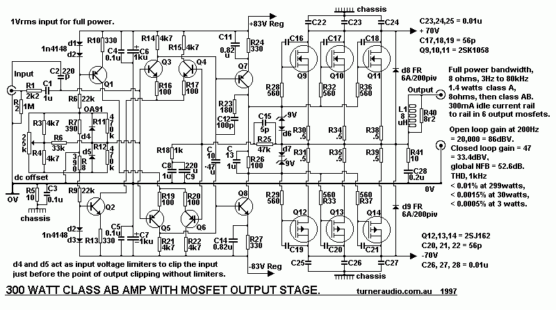
There are six mosfets per channel in the output in complementary
source follower
mode.
The driver stage is also a complementary pair but with BF469/470
bjts in common
emitter mode for high gain. The collector load of each bjt is the
load for the other
of the pair and gain is very high in this simple driver stage.
There are two differential input stages, one npn and the other
pnp.
But they are not cascaded, but coupled to work in parallel to give
wide bandwidth,
low thd and symmetrical square wave performance to a high
frequency.
I found BF469 and BF470 were quite OK to use in the input and
driver stages.
Each of the aluminium extruded heatsinks for the flat pack mosfets
are 300mm long,
150mm high with 30 fins 40mm long, good for a 2 x 300W amp with no
need
for a fan even when left running at 300W into 4r0 with a sine
wave.
The total surface area of the heatsink is 30 x 15 x 4 x 2 = 3,600
square cm.
The required surface area needed to keep T rise less than 40C
approx is
about 40 sq.cm per W, so the extruded heatsinks I used are good
for 90W
of dissipation, or a lot more if one allows for a higher T rise.
If anyone follows my
simple rules here they should find their amps won't run hot, but
the heatsink fins
MUST be vertical, and not within a box which restricts air flow,
and causes rise.
Devices should be fixed to the heatsink with machine screws and
heat paste
and be spread over the area of the backing plate of the sink.
The 150mm x 300mm x 30 fin sink would be good for a 40W pure class
A amp which
needs to dissipate 90W at idle to allow 40W of class A.
I have thermal fuses fitted
to each heatsink to shut the amp down if the temperature exceeds
76C, but I have
never been able to trigger the fuse. I biased each channel it for
about 42W of idle
dissipation ( 300mA idle current ) which gives about 1.4W of class
A before moving
to class AB for the next 250W into 8 ohms. The high bias currents
in the mosfets stops
all tendencies of the mosfets to oscillate at RF where idle
currents are low, as used in
BJT amps.
The schematic is about as simple as a good 300W solid state amp
can be.
All the input driver bjts are mounted on a strip of aluminium
above the board to
keep them all at about the same temperature.
There is limiting of the input voltage to prevent excessive
accidental input voltage
being applied.
There is a decent protection circuit on the output used which
isn't shown, which
turns off the amp if there is a dc offset fault that exceeds about
+/- 1V for longer
than 4 seconds. The 0.5 ohm "N" source resistors are non magnetic
wire wound
types to prevent oscillations and force the mosfets to share the
the current evenly
and remain evenly biased without great need for the mosfets to be
accurately matched.
Anyone trying to build an amp with mosfet output devices should
anticipate parasitic
oscillations at RF. I found that 56pF from gate to drain with
short leads plus 560
ohm gate "stoppers" on each mosfet eliminated the RF oscillations.
I also have four
bypassing caps. The power supply has large 75V rated Sprague
100,000uF capacitors
on each +/- 70V rail, but the leads from the caps have enough
inductance to prevent
silent rails when testing with square waves so I placed 1,000 uF
electros + 0.47 uF
with short leads from the drain rails to 0V, then one 0.01uF from
each drain to the
chassis, and finally there was no more rail signal present at HF.
The open loop bandwidth is maximum at 200Hz but -3dB at about 5
kHz with only
180 ohms plus 100pF ( R23/C12 ) needed from the driver collectors
to bases of
Q7+Q8 to tailor the open loop phase and gain to stop overshoot and
HF instability.
In addition there is the C15 across R25, 47k to compensate for the
open loop phase
lag at HF. The RC zobel network R41+C28 from the commoned sources
to 0V act
to provide the amplifier with a resistive load above 100kHz when
the 0.22uF cap has
an impedance of 7.3 ohms. At F above 200kHz, the load on the
output stage is 10
ohms if there is not other load connected so the amp is more
likely to remain stable.
The value of C15 isn't given because in my case it was a pair of
short insulated
wires twisted together until the stability became excellent. A
trim cap of 3 to 20pF
could be used.
With 6r0 load, each mosfet sees 36r0 while in class A and then
18r0 when in class AB.
So while in class A the gain reduction in the output stage with
follower action is about
from 25 to about 1, and this local source follower series voltage
FB totals about 27dB.
The output stage works mainly in class AB and in fact not much
different to a class
B amp where there is no idle current at all. With no source
follower or global NFB
the THD of a pair of mosfets in complementary pair might be 10% at
250W to 8r0.
The 27dB of local NFB used in the source follower connection
reduces this to less than
1%. There is about 50dB of global NFB which means a total of 77dB
is operative.
The driver stage, Q7+Q8, has to produce a voltage slightly higher
than the speaker
output voltage and its open loop THD at about 45Vrms is about 3%
of which most is 3H
followed by 2H. This adds to the output stage THD to make a grand
total of about 4%
THD with no global NFB.
Most of the crossover distortion artefacts are reduced by the
local output stage NFB.
The 53dB of global FB reduces the 4% open loop THD by 53dB, or by
a factor of
0.00223, so 4% becomes 0.0089%, or just under 0.01%.
The THD is approximately proportional to the output voltage, and
at 4.5Vrms output
which is 2.5W / 8r0, THD < 0.001%, and rather difficult to
measure easily.
Such low THD is typical of many solid state amplifiers. However,
excellent THD, IMD
and TID measurements do not always tell the whole story about how
an amplifier will or
will not alter the sound signals than pass through it.
Tube amps with ten times the THD can sound better.
(( And by the way, anyone could operate the 300W amp design as a
pure class A
amp by having say 2 more output devices and dissipating about 80W
at idle,
and then using +/- 35Vdc rails instead of +/- 70Vdc. You could get
up to 36W pure class A,
depending on the load value. The same input stages and driver
stages would produce
about 3% open loop thd, and need some global NFB to reduce it. It
would not measure
much better than the above low bias class AB amp.
Subjectively, The class A operation of the output mosfets may
sound better than
having a 300W capability, which is never fully used. ))
With the class AB 300W amp as it is, any type of load can be
connected and an
8 uH inductance in parallel with 8 ohms protects the output stage
from over heating
if it ever had 5uF connected and the output signal had a high
level signal above 20kHz.
5uF is a difficult load, but there may be some electrostatics,
possibly made by
"Lartin Mogan", which present such an awkward load to an amp, but
usually all
awkward loads do have a series resistance in their equivalent
impedance
characteristic so that the worst of phase shifts and peak currents
at above 10kHz will
not bother the amplifier, and in any case the % of audio F energy
above 7 kHz is
usually very small. 5uF = 4.5 ohms at 7 kHz, and 2.27ohms at 14
kHz, and in fact
most amplifiers of any type will cope quite well with such a load
providing the
output voltage levels remains well below the maximum possible
which is probably
going to always be the case with an amp capable of 300W if it is
used for "normal hi-fi"
and with average speakers, which most ppl find sound loud enough
with never any
more than 10 W.
There could be a problem driving 5uF or with with insensitive
electrostatics if the
amplifier was only rated for 10W, and if high levels were wanted.
Quad ESL57 are
equivalent approximately to 1r6 in series with 2uF with 16r0
across the 1r6+2uF also
as a load. The response peaking effects caused by 2uF as the sole
load are usually
prevented by the series R in front of the C; the other 16r0
has little loading effect at all, and in fact ESL57 are very easy
loads to drive by
my 300W amp or any other amp. However, Quad's later model, the
Quad 63
and following models need more than a 20W amp.
There is current limiting that operates to prevent the output
stage from developing
excessive current which is dangerous to solid state devices which
can very rapidly
fail if the excessive current lasts for long enough to heat them
up and fuse the small
pn junction size of the active devices which are not much bigger
than a 4mm x 4mm
area.
Tubes have large metal areas
of perhaps 12sq.cm, ( EL34 ) and temporary adverse heat
dissipation can be
tolerated for longer than in a solid device.
The maximum theoretical peak load current = rail voltage / (
load + Ron + Rs )
where Ron is the minimum 'on' resistance of the mosfet when fully
turned on,
Rs = the source resistor. In this case if RL = 3r5, load on each
mosfet = 10r5,
Ron = 1r0 and Rs = 0.5r, so I max = 70V / 12r0 = 5.8Apk.
The rating for the mosfets is 7Apk.
The voltage gain of the mosfets reduces with RL value so a single
mosfet with
a 10r5 load plus Rs 0.5r will have a Vac change of 0V to +63.8Vpk,
and the Vg-s change needed is about +8V. There will be 2.9V across
the 0.5r Rs,
and the 9V zener diode plus other diode will conduct to prevent
any increase in
signal at the gates from over driving the mosfet.
To cut a long story short, in effect, the maximum current able to
be produced by the
amp = 14Apk for 3 mosfets, and in fact my measurements indicate
maximum load
current cannot be any higher than when load = 3r5 or lower, and
the output power
= 350W. So with 1r0 load there is still 14Apk peak produced, and
maximum output
power is about 100W.
The amplifier would become overheated with a load of 1r0 and
worked hard but
then the fuses in rails or at the output ( not shown ) would blow.
The amp is meant
to be used with loads above 4r0, but will tolerate normal home use
with loads down
to 2r0 where power is unlikely to average more than 3W per
channel, ever.
The only way to increase low impedance speaker load power handling
is to use
more of the same output devices or use devices with higher ratings
and more
of them on a bigger heatsink. Exicon flat pack mosfets rated for
16A each,
which would allow 40Vrms into 2r0 giving 800W.
I have never ever needed more than 50W for hi-fi at home.
There is an input voltage limiting circuit included which prevents
excessive input
voltages from being applied to the input transistors. Diodes D4
and D5 act to
shunt excessive input voltage just before the amp output stage
clips.
Below clipping the input limiters have zero action on the input
signal because each
diode which is a fast type with low forward turn on voltage
<0.25V is biased by
the resistance networks.
The input limiting may be omitted if really wish, but if used it
requires very
careful setting up to avoid any input clipping below high power
levels.
The amp has been reliable and trouble free and was a great
learning exercise to
build. I have surreptitiously substituted it for a 50W PP class A
tube amp during a
demonstration in about 1999, and the 3 other guys present did not
hear any noticeable
change. However, I had poorer speakers in those times using cheap
asian made drivers.
The speakers I have built since then use far better sounding SEAS
drive units and much
better enclosures and perhaps I now would not get away with
playing such skullduggery
on unsuspecting audiophiles.
Maximum output voltage is about 45Vrms. It is possible to use such
an amp in pure class A.
The bias Idc rail to rail may be increased to about 500mAdc, so
that about 70W may be
dissipated in each heatsink.
Using a toroidal audio transformer with 3 : 1 step down ratio, the
45Vrms is reduced to
15Vrms which will give 34W of pure class A into 6r6.
All power into loads above 6r6 will be pure class A.
There will be 75W class AB into 3r0 with initial 13W pure class
A.
A suitable toroidal is made by the man at www.zeroimpedance.com in
the USA.
When I wound the power transformer I used 4 x 25Vrms secondaries
all in series
to give 50V-0-50V which produces +/-70Vdc rails. The 25V rails
could be
paralleled to allow +/- 35V rails. The six mosfets could still
dissipate 70W but
be able to put 32W of pure class A into 16r0, 60W class AB into
8r0, including 16W
class A, 100W of class AB into 4r0 with 8W class A.
The measured distortion would become extremely low at audiophile
levels of power,
and perhaps the class A would convey some better subjective
fidelity.
People told me why my tube amps and mosfet amps both sound well.
One reason
is that they run warm without the devices being under stress and
do not run so hot
that devices will be short lived. My PP amps have always given
enough initial class A
power rather than hardly any at all. Friends were not able to tell
the difference between
my SS amps and tube amps in blind AB tests I did, and didn't mind
this because the
same guy was using similar philosophy for whatever he made.
One friend I had 4r0 Duntech Sovereign speakers which were huge
floor standing
units with many drivers. They could achieve astonishing sound
levels.
My friend played a vinyl
recording of 20 Africans beating away on drums and percussive
instruments thus generating a very "difficult" and transient rich
signal. We were able
to just get my 300W amp into clipping on the transients but the
outcome sounded
exactly like 20 Africans belting away furiously on leather and
wood. Of course such
levels could not be sustained or neighbours would call the police
control.
Some Lieder music from old Europe also sounded detailed and sweet,
and methinks
the 'Elephant' treads softly when required.
300W amp power supply.
Underside 2 x 300W amp.
Back to Index page